|
Product Features:
- 320X256 Array Format
- 28-pin Metal DIP Package
- Embedded Thermoelectric Cooler
- 0.9 μm – 1.7 μm Spectral Range
- Typical Pixel Operability > 99.5%
- Quantum Efficiency > 70%
Applications:
- Near-Infrared Imaging
- Imaging Spectroscopy
- Covert Surveillance
- Medical Science and Biology
SPECIFICATIONS (ITS = 25ºC):
Parameters
|
Symbol
|
Test conditions
|
Min
|
Typ |
Max
|
Unit |
Sensor Technology
|
|
|
Standard InGaAs/InP
|
|
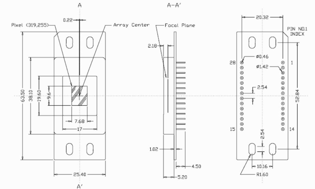
Image Format
|
|
|
320(H)x256(V)
|
|
Image Size
|
|
|
9.6(H)x7.68(V)
|
mm
|
Pixel Pitch
|
|
|
30x30 (>99% Fill Factor)
|
µm
|
Spectral Response Range
|
λ
|
|
900
|
|
1700
|
nm
|
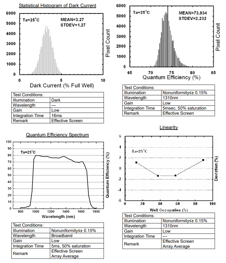
Dark Current
|
|
Pixel bias @ 0.1V
|
|
|
0.4
|
pA
|
Quantum Efficiency
|
|
λ = 1.0~1.6µm
|
70 |
|
|
%
|
Fill Factor
|
|
|
99 |
|
|
%
|
Adjacent Pixel Crosstalk
|
|
|
|
|
1
|
%
|
Detectivity
|
|
Tint=16ms, High Gain λ = 1.55µm
|
5X10¹² |
|
|
Jones
|
Response Nonuniformity
|
|
Under 50% Saturation
|
|
|
10
|
%
|
Nonlinearity
(Max. Deviation)
|
|
Over 10%-90% Full Well Capacity
|
|
|
2
|
%
|
Max. Pixel Rate
|
|
|
|
10
|
|
MHz
|
Gain
|
|
|
0.7
|
|
13.3 |
uV/e-
|
Full Well
|
|
|
High: 170K e- / Low: 3.5M e-
|
|
Pixel Operability(*)
|
|
Dark Current ≤20% Full Well Response Nonuniformity ≤ 20% |
99
|
|
|
%
|
Image Size
|
|
|
9.6 x 7.68
|
mm
|
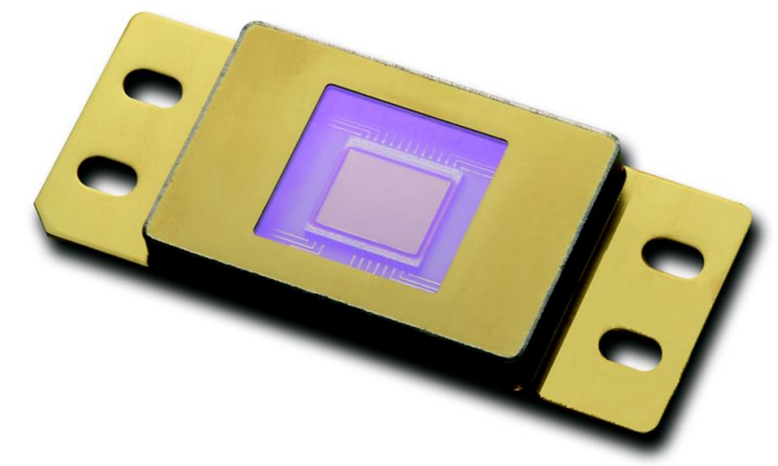
Package Type
|
|
|
28-pin Metal DIP Package
|
|
Weight
|
|
|
24.6
|
g
|
Note (*): Pixel Operability is defined within the center 318x254 regions.
Absolute Maximum Ratings :
| |
Parameters
|
Min
|
Typ |
Max
|
Unit |
| |
Operating Temperature
|
-20
|
|
85
|
°C
|
| |
Storage Temperature
|
-40
|
|
85
|
°C
|
| |
Power Consumption (*)
|
|
|
175
|
mW
|
Note (*): Without driving the cooler.
Package Dimensions (mm):
Bias Input :
| |
Pin #
|
Bias
|
Voltage |
Current
|
Remark |
| |
12
|
VPD
|
5.5V |
<1mA
|
Logic positive supply
|
| |
13
|
VND
|
0V |
<1mA
|
Logic negative supply
|
| |
21
|
VPOSOUT
|
5.5V |
<25mA
|
Output stage analog supply
|
| |
15
|
VNEGOUT
|
0V |
<25mA
|
Output stage analog ground
|
| |
1
|
VPOS
|
5.5V |
<5mA
|
Positive analog supply
|
| |
28
|
VNEG
|
0V |
<15mA
|
Negative analog supply and
substrate
|
| |
4
|
VPOS_CORE
|
5.5V |
<15mA
|
CTIA amplifier positive supply
|
| |
2
|
VDETCOM
|
4.7V~5.5V |
<5mA
|
Detector common voltage
Detector bias = VDETCOM-4.7(*)
|
Note (*): VDETCOM lower than 4.7V will forward bias the sensor, the exact zero bias voltage is device and
temperature dependent.
Digital Pattern Input :
| |
Pin #
|
Clocks
|
Levels |
Rise/Fall
|
Remark |
| |
11
|
CLK
|
0V~5.5V |
<10ns
|
Master clock Max. Freq.=5MHz
|
| |
9
|
FSYNC
|
0V~5.5V |
<10ns
|
Frame sync - controls frame start and
integration time
|
| |
10
|
LSYNC
|
0V~5.5V |
<10ns
|
Line sync - controls line readout
timing
|
| |
8
|
DATA
|
0V~5.5V |
<10ns
|
Data code input - programs device
function registers in Control Mode
Left open in Default Mode
|
| |
Clocks
|
Synchronization |
| |
FSYNC
|
Rising and falling when CLK is rising
|
| |
LSYNC
|
Rising and falling when CLK is falling
|
| |
DATA
|
Rising and falling when CLK is rising
|
Video Output :
| |
Pin #
|
Outputs
|
Levels |
Settle
|
Remark |
| |
16
|
OUTA
|
1.3V to 4.2V |
<50ns to
0.1%
|
Output A used in single output
mode
|
| |
17
|
OUTB
|
1.3V to 4.2V |
<50ns to
0.1%
|
Output A and B used in two
output mode
|
| |
18
|
OUTC
|
1.3V to 4.2V |
<50ns to
0.1%
|
Output A, B, C, and D used in
four output mode
|
| |
19
|
OUTD
|
1.3V to 4.2V |
<50ns to
0.1%
|
Output A, B, C, and D used in
four output mode
|
| |
20
|
OUTR
|
3V |
|
Reference for common mode
output
|
Gain & Bandwidth Selection in Default Mode :
| |
Pin #
|
Functions
|
Low |
High
|
Remark |
| |
7
|
GAIN
|
0V / C=10fF |
5.5V / C=210fF
|
Selects unit cell integration
capacitor
Left open in Control Mode |
| |
6
|
BWL
|
0V / Low BW |
5.5V / High BW
|
Selects bandwidth limiting capacitor
in unit cell
Left open in Control Mode |
Advanced Function :
| |
Pin #
|
Functions
|
Voltages |
Remark |
| |
25
|
VCAS(*)
|
3.75V |
CTIA amplifier cascode FET biase |
| |
24
|
VOUTREF(*)
|
3V |
Output reference level during blanking period |
| |
23
|
VBLM(*)
|
2V |
Detector bloom control |
| |
27
|
IMSTR_ADJ(**)
|
0V~5.5V |
Adjusts analog master bias current |
| |
22
|
VOS
|
0V~5.5V |
Variable Offset/Skimming Control Voltage |
| |
5
|
TEMP
|
0V~5.5V |
On chip temperature monitor
0.74V at 300K Slope=-14.8mV/10K in 50-300K |
Note (*): Internally generated after bias input, but can be overridden.
Note (**): Also addressable through control register (DATA).
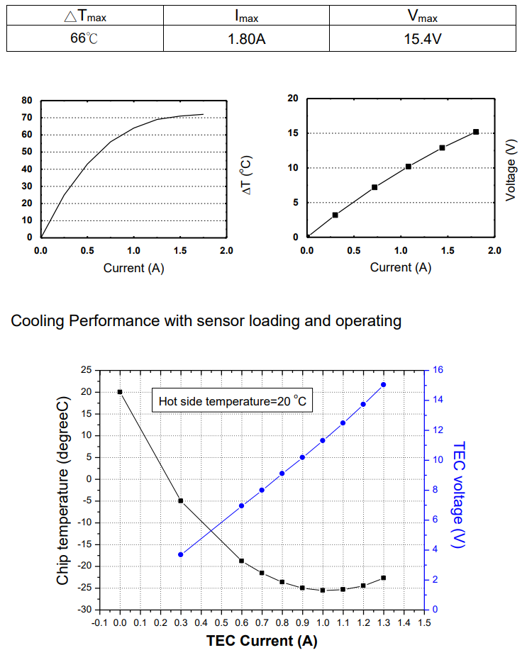
THERMOELECTRIC COOLER DATA (Without thermal loading) :
EXAMPLE CURVES :
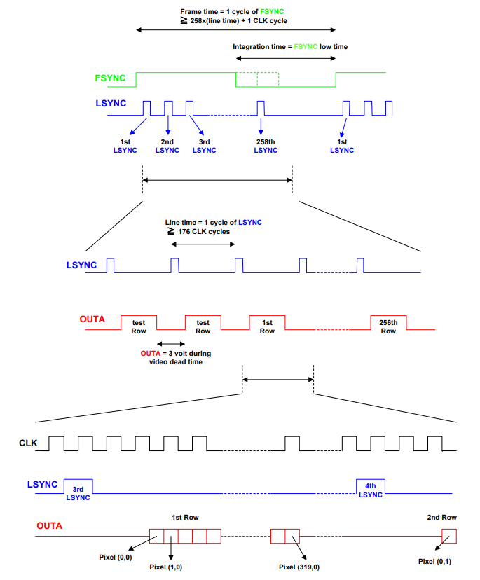
TIMING CHART FOR DEFAULT MODE OPERATION :
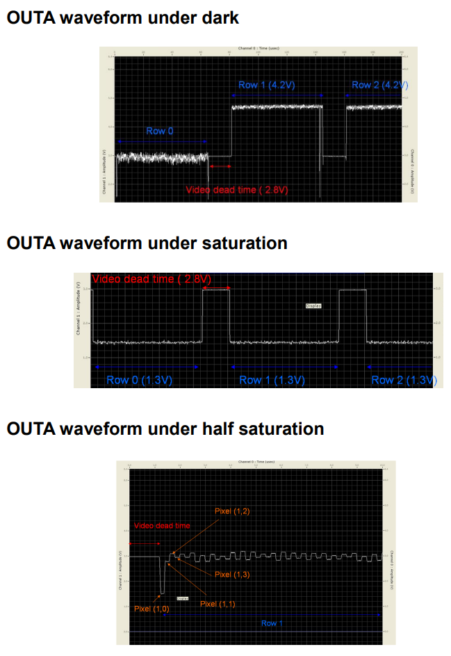
OUTA Waveform :
|